Transient Voltage Suppression Diode: TVS Protection Circuit Guide
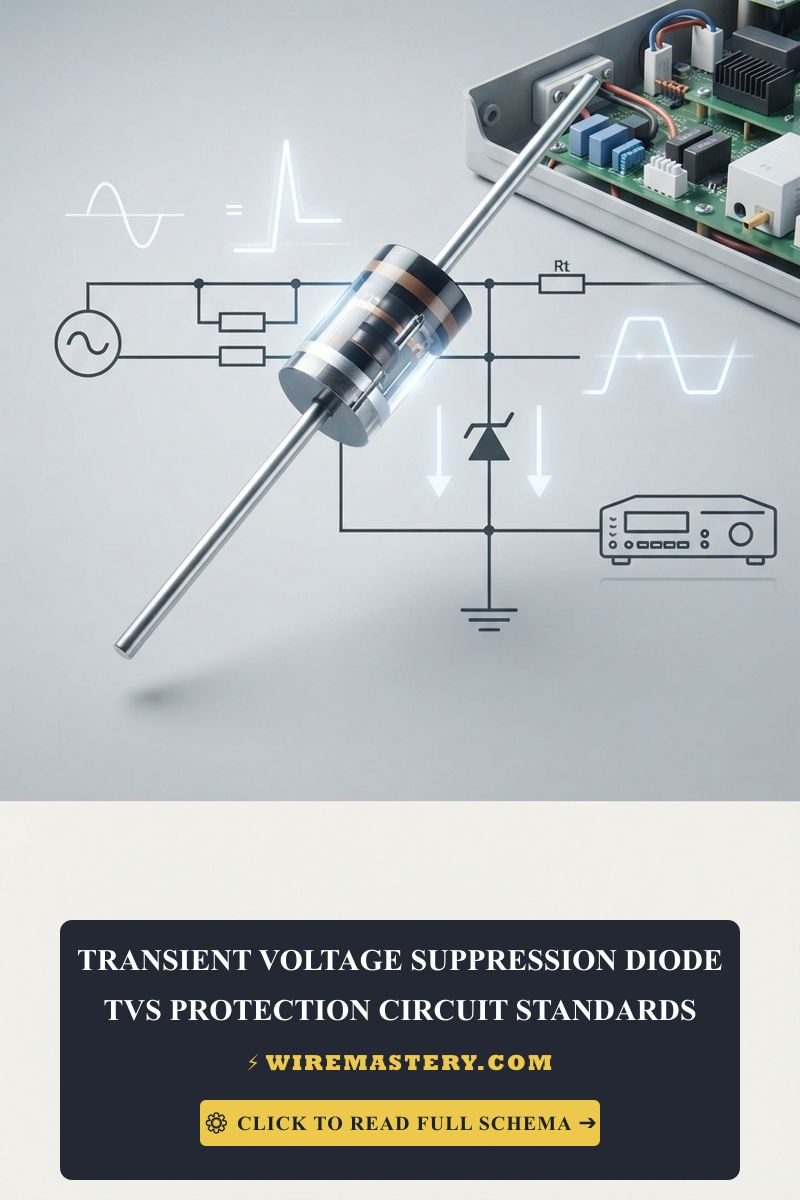
Protecting sensitive microprocessors and solid-state data communication ports against transient voltage spikes is a foundational requirement in modern hardware engineering. High-voltage subsecond transients—triggered by Electrostatic Discharge (ESD), lightning induced inductive coupling, or utility inductive load switching switches—can instantly puncture microchip junctions and compromise smart home nodes. Implementing a dedicated Transient Voltage Suppression (TVS) diode matrix provides an ultra-fast silicon-level clamp that redirects hazardous energy surges safely away from high-density processing lines.
The technical specifications of TVS diodes, clamping voltage parameters under IEC 61000-4-2 standards, and physical printed circuit board (PCB) layout design guidelines.
Core Semiconductor Selection Parameters
Before soldering a protective semiconductor array onto a custom control board, decode these core engineering metrics:
- Response Response Time: TVS diodes feature sub-nanosecond clamping activation speeds (clamping arcs faster than metal oxide varistors or gas discharge tubes).
- Polarity Constraints: You must distinguish between Unidirectional TVS profiles (for DC voltage rails) and Bidirectional profiles (for AC signaling and alternating differential lines).
- Capacitance Limitations: High-speed communication links (like USB 3.0 or Gigabit Ethernet) require ultra-low capacitance TVS footprints (below 1pF) to avoid attenuating the data signal frequency waveform.
Technical Materials & Diagnostic Testing Checklist
Safely auditing and measuring solid-state surge clamping thresholds requires specific electrical engineering bench instrumentation:
| Electronics Lab Instrument | Primary Engineering Purpose |
|---|---|
| Digital Storage Oscilloscope | Captures fast high-frequency nanosecond transient voltage waves to verify diode reaction limits. |
| Auto-Ranging Multimeter | Measures reverse bias leakage current profile and verifies solid-state junction continuity. |
| Regulated DC Bench Power Supply | Delivers step-voltage profiles to determine the exact breakdown limits of the silicon junction. |
| ESD-Safe Soldering Station | Precision temperature-controlled iron to secure micro-component solder pads safely. |
Technical Specifications: The TVS Selection Matrix
Selecting the appropriate TVS diode requires balancing the operational voltage of your protected chip against the maximum clamping thresholds of the semiconductor silicon. Utilizing an incorrect model will either leave your microprocessors unprotected or cause the diode to conduct continuously under normal operating conditions.
To trace how these protective elements integrate with broader hardware nodes, review our comprehensive manual on basic electronic components and circuit design.
Critical TVS Engineering Parameters
| Technical Parameter | Standard Abbreviation | Engineering Definition & Calculation Limit |
|---|---|---|
| Reverse Stand-Off Voltage | V_RWM | The maximum continuous working voltage where the diode remains completely invisible (Open state). |
| Breakdown Voltage | V_BR | The exact point where the silicon junction enters avalanche conduction, beginning to divert current. |
| Clamping Voltage | V_C | The maximum peak voltage allowed to pass through across the diode during a severe high-amperage surge event. |
| Peak Pulse Current | I_PP | The maximum transient surge current rating the device casing can dissipate without suffering physical destruction. |
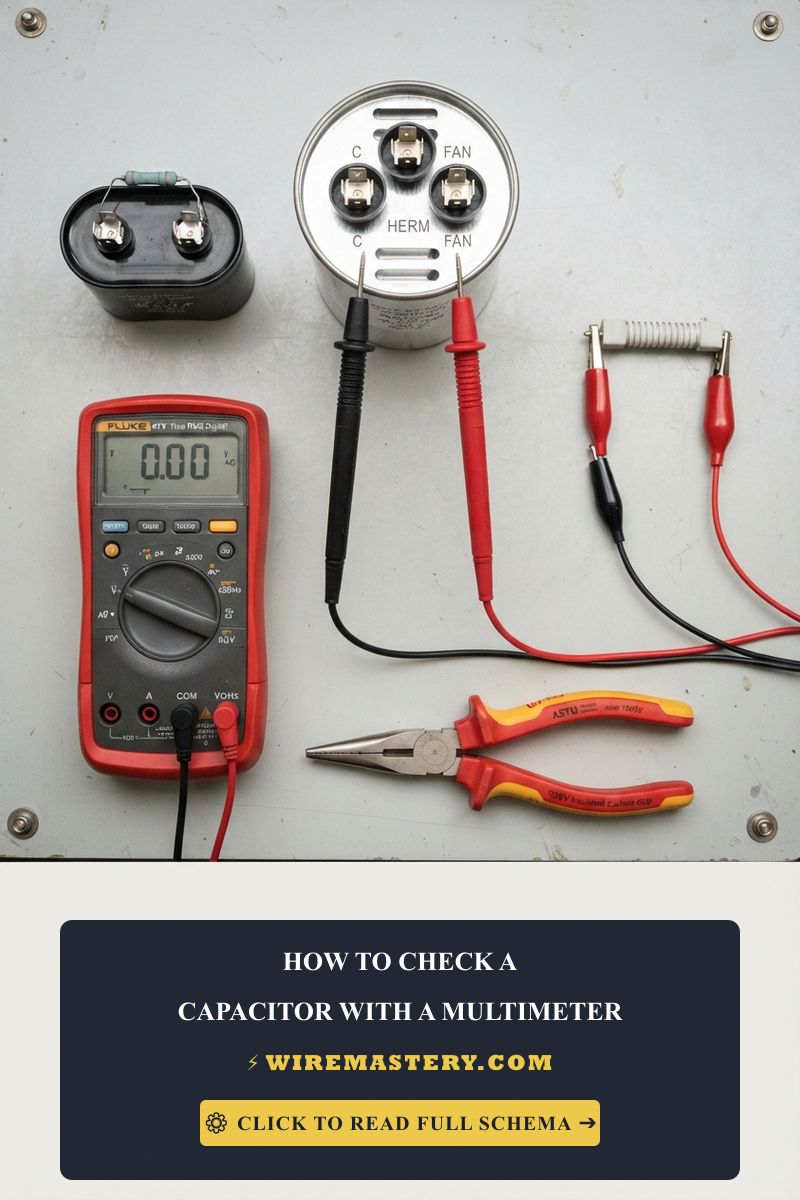
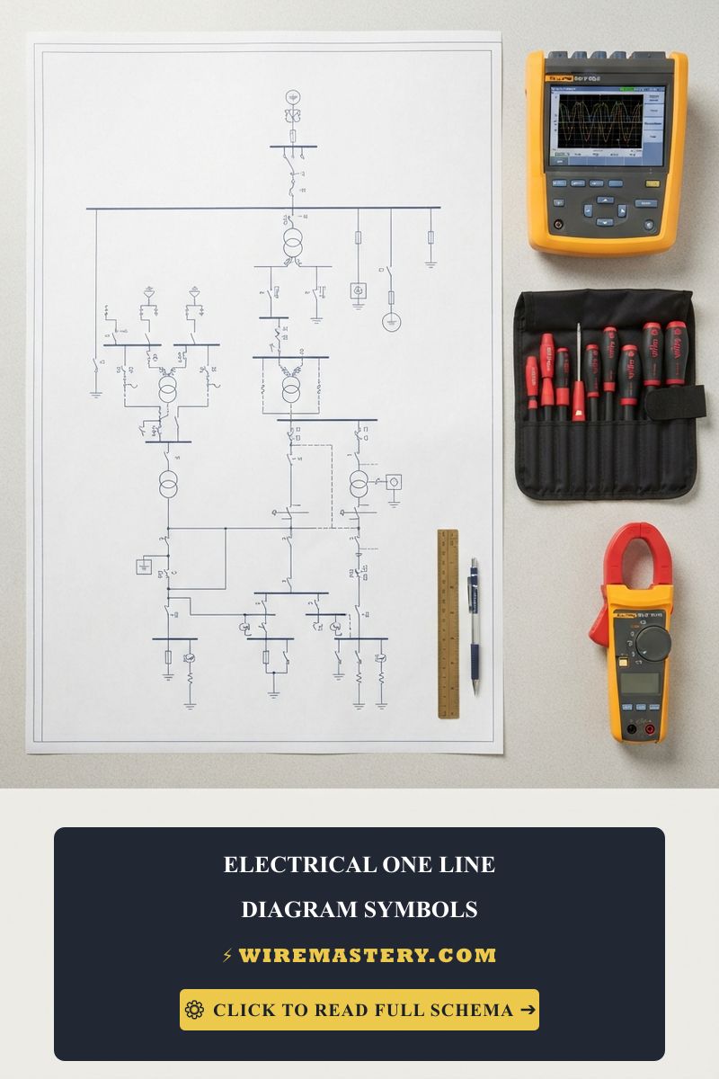
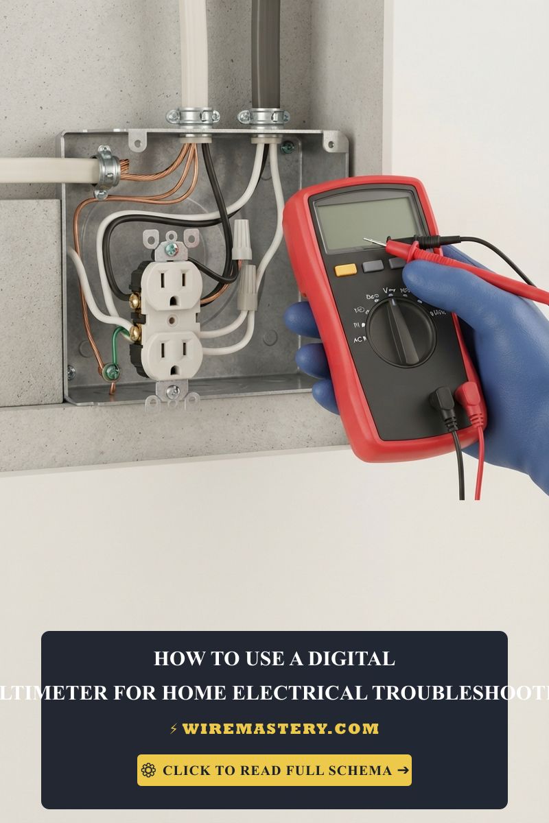
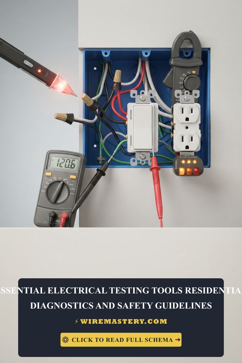
🛠️ Hardware Engineering Check: Look closely at the realistic 3-way layout mockups and device assets displayed across your guide frameworks. Notice how discrete semiconductor protection arrays require compact terminal path mappings. When routing low-voltage data tracks, the TVS diode must be positioned as close to the physical entry connector plug as humanly possible, ensuring the high-energy surge is suppressed before traveling deep into your circuit network loops.
International Surge Immunity & Compliance Standards
Unlike building electrical wiring branches regulated under building codes, solid-state electronic surge safety profiles are governed strictly by international industrial compliance standards:
1. IEC 61000-4-2 (Electrostatic Discharge Immunity)
This standard outlines the circuit’s structural resistance limits against sudden body static discharge sparks. A code-compliant TVS diode must withstand:
- Contact Discharge Testing: Minimum ±8 kV applied directly to conductive metallic terminal blocks.
- Air Discharge Testing: Minimum ±15 kV passing through ambient air slots into user interface zones.
2. IEC 61000-4-5 (Surge Immunity Standards)
Defines the circuit’s threshold capabilities against high-energy lightning-induced transients and power industrial grid switching surges. It utilizes specific 8/20 µs wave pulse currents to measure the absolute clamping efficiency of the silicon boundaries.
Step-by-Step TVS Circuit Layout Implementation Manual
1. Determining the Continuous Rail Voltage
Measure the clean operating direct current (DC) line voltage of the microprocessor port you intend to shield using your digital multimeter. For example, if protecting a standard microcontroller input track, the line runs at 5V DC. Your chosen TVS diode must carry a Reverse Stand-Off Voltage (V_RWM) of exactly 5.0V to avoid interfering with normal processing states.
2. Positioning the Traces on the PCB
When layout routing your printed circuit board (PCB) CAD files, place the TVS pad footprint directly between the external input socket pin and the chip pin. The copper line path must pass through the TVS pad first. Ensure your ground return track is extra wide, short, and low-impedance to allow the transient surge current to exit the board framework into the system earth line instantly.
3. Executing Low-Thermal Soldering Terminations
Because miniature TVS diodes (such as SOT-23 or SMA surface-mount packages) feature thin silicon wafers, excessive heat during soldering will induce permanent lattice defects inside the junction.
- Set your ESD-safe soldering station to exactly 350°F (176°C).
- Apply a microscopic bead of flux to the PCB copper pads.
- Secure one terminal pin using low-residue lead-free solder wire within 2 to 3 seconds max, allowing the package to cool down fully before terminating opposing pins.
Troubleshooting Solid-State Protection Failures
- The TVS Diode Has Become a Permanent Short Circuit: This behavior indicates the transient surge exceeded the diode’s maximum Peak Pulse Power (P_PK) limits. When a TVS diode fails, it sacrificial-shields your system by dropping dead into a direct short-to-ground state to save the expensive main microcontroller chip. Replace the component with a higher I_PP rated model immediately.
- Data Signals Are Distorted or Dropping Packets: This occurs when an installer selects a standard high-capacitance power-rail TVS diode for high-frequency signal lines. The diode’s internal capacitance acts as a high-pass filter, flattening the sharp digital square waves. Swap out the device for an ultra-low capacitance TVS variant (below 0.5pF).
- The Protected Chip Suffered Damage Anyway: Check your ground loop traces. If your PCB ground line is long or narrow, the inductive resistance will generate a secondary voltage spike inside the board walls, completely bypassing the diode’s clamping capabilities.
National Electrical Code Infrastructure Alignment
While small low-voltage Class 2 signal circuits operating inside electronic devices do not fall under the branch circuit safety inspections of the National Electrical Code (NEC), any micro-automation controller connected to industrial grid systems must maintain code-compliant physical separation thresholds. Under NEC Article 725, all low-voltage microelectronic data lines must maintain a minimum 2-inch clear physical separation from high-voltage 120V/240V residential power line branches inside electrical junction boxes to prevent accidental arc induction hazards from frying your smart automation boards.
For current NFPA 70 guidance relevant to surge protection, equipment grounding, transient-voltage suppression, and installation requirements, consult the Official NFPA 70: National Electrical Code (NEC).
Conclusion
Successfully integrating a transient voltage suppression diode matrix into your smart automation circuits safeguards sensitive silicon microprocessors against unpredictable grid surges and body static ESD hazards. By matching stand-off voltages to your operational rails, selecting ultra-low capacitance footprints for your data paths, and enforcing clean high-frequency PCB ground tracking, you build a resilient, automation network. Prioritize fast-clamping design validation, protect modules from static discharge dropouts, and design every circuit with systematic precision.