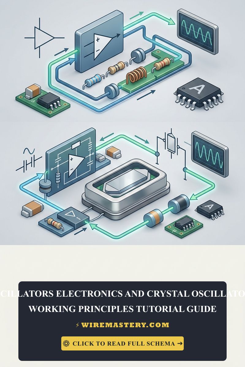
Oscillators in Electronics: Crystal Oscillator Principles
Designing and auditing stable high-frequency clock generation networks within digital processing systems or radio-frequency (RF) transceivers demands a comprehensive understanding of feedback thermodynamics, solid-state circuit parameters, and mechanical quartz resonance physics. Operating as the primary metronome for microcontrollers and embedded logic architectures, an oscillator circuit translates continuous direct current (DC) energy into a clean, repetitive alternating current (AC) waveform—such as a non-linear square wave or a low-distortion sine wave. When configuring these high-speed signal tracks, minimizing jitter and phase noise is critical; any drift in clock integrity will corrupt data serialization routines. To prevent external high-voltage transient spikes from infiltrating and fracturing these delicate logic timing planes, engineering best practices demand buffering your main sub-system traces using a specialized transient voltage suppression TVS diode protection network.
This reference manual outlines the mathematical logic of sustained oscillation loop gains, the mechanical physics of quartz cuts, and advanced electronic laboratory diagnostic workflows.
Core Oscillator Engineering Thresholds
Before placing high-frequency component paths onto a prototyping board or routing fine signal traces, establish these core hardware parameters:
- The Barkhausen Criterion: For any analog active loop to achieve and sustain automatic, unbroken oscillation, the total mathematical loop gain (beta A) must be exactly equal to or greater than Unity (1.0 or 0 dB), and the cumulative phase shift around the closed feedback loop track must evaluate to an exact multiple of 360° (or 0°).
- The Piezoelectric Effect Paradigm: Quartz crystal units utilize inverse piezoelectric physics. Applying an alternating electrical potential across the physical faces of a precision-cut quartz wafer induces a physical, mechanical deformation wave that mirrors the signal frequency exactly.
- The Quality Factor (Q) Variance: Standard discrete resistor-capacitor (RC) or inductor-capacitor (LC) tank networks yield a low Quality Factor (Q ~100), causing progressive frequency drift under ambient temperature shifts. In stark contrast, mechanical quartz resonators achieve extreme stability levels with a high Quality Factor (Q ~10,000 to 100,000).
Technical Materials & High-Frequency Electronics Laboratory Toolkit
Safely building, decoupling, and visualizing ultra-fast digital square waves requires specific electronics laboratory instrumentation and high-precision trade tools:
| Electronics Lab Instrument | Primary Engineering Purpose & Application Spectrum |
|---|---|
| Digital Storage Oscilloscope (DSO) | Minimum 200 MHz bandwidth equipped with low-capacitance active probes to visualize true waveforms. |
| RF Vector Network Analyzer (VNA) | Measures internal crystal equivalent series resistance (ESR) and motional capacitance steps. |
| Regulated Bench DC Power Supply | Delivers low-noise, ripple-free continuous voltage loops (3.3V or 5.0V) to drive active gates. |
| Temperature-Controlled Soldering Station | Precision fine-tip iron certified under ESD guidelines to mount delicate crystals without thermal stress. |
| Anti-Static ESD Grounding Mat & Strap | Dissipates body static charges safely away to prevent punching through microchip oxide layers. |
Sizing Conductor Gauges & Trace Impedance Boundaries
When routing high-frequency oscillator signal lines or supplying power to active logic inverter chips, standard high-voltage residential wiring conventions are completely irrelevant. Instead, engineers adhere strictly to IEEE signal tracking and PCB layout design criteria:
- 22 AWG to 26 AWG Solid Conductor (Signal Benchmark): Standard thickness parameters reserved for low-power bench prototyping wire hookups and signal data patch runs.
- The Guard Ring Trace Layout Requirement: High-frequency crystal lines are highly sensitive to external electromagnetic cross-talk. Layout engineers surround the raw crystal copper traces with a continuous ground plane trace known as a guard ring. This shielding structure sinks stray parasitic capacitance signals straight to the system ground plane before they can distort the main clock frequency.
Deep-Dive: The Mechanical Engineering of Quartz Resonator Cuts
The fundamental resonant frequency and thermal drift coefficient of a crystal oscillator are not determined by software logic, but by the precise mechanical angle at which the raw quartz crystal slab was sliced relative to its crystallographic axes:
1. The AT-Cut Crystal Configuration (The Industry Benchmark)
The AT-Cut represents the most widely deployed crystal profile inside modern consumer and industrial electronics microchips.
- The Geometry: Sliced at a precise orientation angle of approximately 35° 15’ relative to the quartz Z-axis optical plane.
- The Thermodynamic Advantage: The AT-cut wafer vibrates in a thickness-shear mechanical mode. This unique geometric profile results in an incredibly stable temperature-coefficient curve, ensuring the oscillator frequency stays flat across standard operational windows spanning from -40°C up to +85°C.
2. The Fundamental vs. Overtone Operational Modes
- Fundamental Mode: The crystal wafer physical thickness dictates the base speed. Standard manufacturing techniques limit fundamental mode crystals to a maximum frequency threshold of roughly 30 MHz to 40 MHz; slicing the quartz wafer any thinner makes the glass too fragile to survive physical vibration cycles.
- Overtone Mode: To launch frequencies past 40 MHz up into the hundreds of Megahertz spectrum without cracking the glass, engineers program the active drive circuit to trap the third, fifth, or seventh mechanical harmonic of the crystal (the overtones). This technique unlocks extreme clock speeds while maintaining a robust physical quartz structural integrity.
Advanced Hardware Design: Calculating Load Capacitance
A quartz crystal cannot swing at its true specified resonant frequency as a standalone unit. It requires an external capacitive environment to satisfy the phase-shift logic of the feedback loop.
The Pierce Oscillator Layout
In standard microcontroller design, the internal logic gate pairs with two discrete ceramic capacitors (C1 and C2) running to ground.
-
The Sizing Equation: To determine the correct nominal values for these capacitors, you must execute the standard load capacitance mathematical formula:
C_L = (C1 × C2) / (C1 + C2) + C_s
Where:
- C_L: The absolute target load capacitance explicitly specified by the crystal manufacturer data sheet (typically 12 pF to 20 pF).
- C_s: The parasitic stray capacitance naturally present across the physical copper PCB traces and microchip pins (typically estimated between 3 pF and 5 pF).
- Engineering Consequence: Under-sizing these external capacitors will cause the crystal to vibrate too fast, drifting your clock timing tracks forward. Over-sizing them will starve the feedback loop of gain, preventing the oscillator from launching entirely.
🛠️ Decoupling Trace Design Note: Look closely at the high-density micro-electronic schematic layouts displayed throughout our hardware integration manuals. Notice that active inverter chips generate sudden current spikes whenever they transition logic states (0 to 1). Always place a 0.1µF ceramic decoupling capacitor as close as physically possible to the active device power pins, running straight down to the ground plane layer. This layout element dampens fast line noise, preventing supply ripples from destabilizing the sensitive crystal analog feedback network.
Technical Phase: Conducting a High-Frequency Waveform Audit
To verify the amplitude integrity and frequency stability of an active clock network, engineers perform an in-circuit diagnostic sweep using a digital storage oscilloscope (DSO). For a comprehensive breakdown of the active solid-state amplification layers driving these loops, cross-reference our foundational blueprint on BJT transistor working principles and switching circuit manuals.
The Low-Capacitance Oscilloscope Probe Matrix
- Power up your prototype clock network using a regulated, ripple-free +3.3V DC bench power supply rail.
- Take your oscilloscope probe and verify it is set to the 10x Attenuation position. Never probe a crystal pin using a standard 1x probe layout; a 1x probe introduces massive input capacitance (~100 pF) that will instantly choke the low-power feedback loop, halting the oscillation you are trying to measure.
- Clamp the probe’s short ground lead directly to the nearest system ground plane pin. Touch the needle tip to the Crystal Input (XTAL_IN) trace.
- Analyze the Digital Waveform Output Parameters:
- The System Registers a Flat 0V Line: The loop gain is below Unity or the crystal has suffered mechanical fracture damage. The circuit logic is dead.
- The Screen Displays a Clean, Continuous Waveform: Adjust the time-base dial to match the expected frequency (e.g., 16.00 MHz). Verify the peak-to-peak voltage (V_pp) matches the active logic levels and check that the waveform displays zero jitter distortions or clipping harmonics, confirming absolute clock stability.
Troubleshooting Common Oscillator Circuit Failures
- The Crystal Oscillates on Startup but Dies Intermittently: This behavior indicates high Equivalent Series Resistance (ESR) saturation or moisture contamination across the quartz housing pins. If your soldering technique left conductive flux residue bridging the fine trace gaps, a parasitic leakage path forms, dropping loop gain below the Barkhausen threshold. Flush the circuit board face thoroughly using an electronics-grade dielectric contact cleaner solvent.
- The Clock Frequency Drifts Drastically Under Load: An absolute symptom of thermal over-driving. If the drive level (DL) parameter configured by your active amplifier circuit exceeds the maximum wattage rating specified by the crystal data sheet (typically measured in microwatts, µW), the quartz crystal will physically overheat. This stress warps its mechanical dimensions, inducing rapid frequency drift and accelerating permanent crystal lattice degradation.
- The Microcontroller Fails to boot completely: Check for an active open-circuit fault or reversed crystal input pins. If your trace paths are too long, the trace lines act as antennas, absorbing electromagnetic interference (EMI) from nearby high-current switching rails. Keep your oscillator traces completely isolated, short, and enclosed within an un-broken ground plane wrap.
High-Frequency Signal Isolation Compliance Standards
Adhering to strict international design regulations shields your micro-automation systems from data corruption and ensures full property safety compliance. Because oscillators are low-power micro-signal components, residential high-voltage electrical codes are completely separate; instead, development infrastructures are strictly governed by IEEE and FCC Electronic Compatibility (EMC) regulations:
- FCC Part 15 Component Compliance: Every high-frequency electronic device generating digital clock signals must pass strict electromagnetic compatibility testing to confirm its unshielded radio frequency emissions stay below maximum legal boundaries. This regulation ensures your smart home automated hubs do not bleed inductive noise that jams adjacent aviation or cellular networks.
- ESD Protection Boundaries (IEEE 1686): Oscillator networks must be structurally isolated from external high-voltage static discharges. Integrating dedicated ground planes and utilizing ESD-suppression diodes on all user-facing inputs blocks high-voltage spikes from fracturing delicate semiconductor micro-hardware.
For current IEEE guidance on oscillator design, crystal stability, frequency control, and high-frequency electronics, consult the Official IEEE Standards Association Database.
Conclusion
This guide covers calculating Pierce oscillator load capacitance margins, interpreting AT-cut mechanical shearing thermodynamics, and verifying digital square waves using low-capacitance oscilloscope probes transforms complex clock network troubleshooting into a highly predictable, systematic science. By keeping loop gains strictly above the Barkhausen unity threshold, routing shielded guard rings around fine copper crystal traces, and respecting mandatory FCC Part 15 electromagnetic emission boundaries, you build incredibly resilient, commercial-grade technology frameworks. For final checks, complete benchtop electrostatic discharge isolation protocols, deploy certified high-bandwidth testing instrumentation, and design every micro-signal loop with precision.